Table of Content
The Google Home Mini PCB + Interposer Board can be connected to the NandBug Main Board. As it must be soldered like a BGA component, I'll turn it into one by soldering tiny solder balls. First things first, the NAND Flash must be desoldered from the Google Home PCB. This has been done with a cheap hot air reworking station. It's a model that can be bought from many places and that has served me well for several years now. A small connector matching the one of the main board.
Optionally, a NAND Flash can be directly soldered to the board. A FT2232H. This component adds Hi-Speed USB connectivity to the board. Hardware files are available here while the software can be downloaded from here. I made the schematics, Gerber files, and software of NandBug publicly available. The general idea is in fact to make the NAND Flash of the Google Home in-system programmable. It may sound like an over engineered solution and it maybe is.
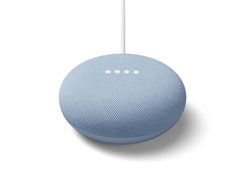
Google Nest Mini
However, The NAND Flash signals are going too fast for achieving this with a simple ICE40 FPGA. This may have been possible with a more advance component. This script will simply generate the Passthrough bitstream and upload it to the FPGA. To generate the needed SPI and GPIO signals, the FT2232H is used in MPSSE Mode.
Repeatedly desoldering and soldering back the NAND Flash would have been annoying and could have caused damage to to the PCB. It's the most direct way of achieving code execution on the platform. My goal will be to modify the NAND flash content until I can execute my own code. The Google Home Mini is protected by some kind of secure boot. Bootloader and Kernel are cryptographically verified. To conclude, at first sight, the hardware looks rather annoying to work with and doesn't appear to be very talkative.
Loa thông minh Google nest mini – Google Home mini thế hệ 2
Receiving and transmitting data to and from the NAND Flash. This is done using the Synchronous FIFO mode of the FT2232H. In this mode, the FPGA and the FT2232H communicates by using a parallel bus synchronized by a 60Mhz clock. The entire content of the 256MB NAND can be dumped in less than a minute. The 60MHz clock is generated by the FT2232H and clock the entire FPGA. The articles highlight that Google has released the source code for the bootloader and Linux Kernel running on the Chromecast.
The Google Home Mini is a smart speaker that's built on the same platform as the original Google Home, but it's significantly smaller. If the device has been used before, factory reset your speaker or display before you continue. The Google Home has a single speaker with two passive radiators, which really help it produce decent sound for a device of its size.
Speaker and microphones
Detailed documentation about this mode can be downloaded from here. Next, the NandBug main board was plugged to a computer and the following command ran. This bitstream will generate a FSM that's able to erase blocks. The addresses to erase are received from the FT2232H using the Sync FIFO Mode. This bitstream implements a simple FSM that will read all pages of the NAND Flash one by one and stream them to the FT2232H using the Sync FIFO Mode. This section gives some information concerning the software and gateware architecture behind NandBug.

A few weeks ago we unveiled Google Home Mini, the newest addition to the Google Home family. About the size of a donut, it has all the smarts of the Google Assistant and gives you hands-free help in any room of your house. Starting today, you can grab it online from the Google Store or online or on shelves of Best Buy, Walmart, Target and other stores.
The first thing to note is that the way the data is written to a NAND Flash is somewhat special. Each page contains data and a special section called OOB, the out-of-bound section. This feature can somehow work a little bit at the very beginning of the Google Home boot sequence though. A this early point, the clock of the NAND Flash peripheral is reduced to a couple of hundred of kHz. More importantly, the Google Home Mini can still boot without problems despite all the heavy surgery it received. Receive the NAND Flash data and compare it to the content of filename.

Both the cache and factory_store partitions are mounted with the noexec flag. Extracting files from this image is just a matter of running the unsquashfs command. For instance, the entire NAND flash layout (i.e. the partitions) can be revealed in the following way.
This source code will be extremely useful in the second article of this series. In 2014, fail0verflow was able to root Chromecast devices with a vulnerability affecting the bootloader. A buffer overflow vulnerability triggered thanks to a special USB peripheral led to a full secure boot bypass. That said, the Home Mini used a micro-USB port instead of a barrel plug connector, and some people preferred that approach.

That information is passed to the cloud, where Google's powerful servers get to work. Don't be fooled by the Google Home Mini's affordable price tag or diminutive size. We know the bootloader and kernel partitions are part of the chain of trust. Unsurprisingly, because they are probably the most carefully written parts, I haven't been able to find any way to skip the secure boot from this side. One of the very early design goal of NandBug was to be able to monitor the data read and written by the Google Home to the NAND Flash in real time. It could maybe have been useful to find interesting TOCTOU bugs in the secure boot implementation.
It's reducing the likelihood I can still discover something to exploit in it to bypass the secure boot on a Google Home Mini. This push button is not accessible without cracking the case open. Pushing it at boot time will force the bootloader to boot from the USB port of the device. However, only signed code can theoretically be executed. The Home tab gives you shortcuts for the things you do most, like playing music or dimming the lights when you want to start a movie.
Once mounted, the cache reveals it's mostly used to store user data and configuration files. For instance, a wpa_supplicant.conf file storing WiFi credentials exists. The connector can finally be hand-soldered to it, using a simple soldering iron. This step doesn't differ much from a "normal" BGA component soldering. The NAND Flash footprint is soaked with solder flux, the Interposer Board carefully aligned to it, and hot air is applied.
Set up your Nest Wifi and Google Wifi in minutes using the Google Home app. Run speed tests, set up a guest network, and easily share your Wi-Fi password with family and friends. Use parental controls like Wi-Fi pause to manage online time for the kids. Automatically prioritize video conferencing and gaming traffic on all devices, or decide which devices to prioritize for all traffic types. Get more insights on your network, whether it’s a notification when a new device joins your network or detailed insights for troubleshooting a poor internet connection. The Google Home app will walk you through the steps to set up your Google Nest or Home speaker or display.
However, before even thinking of patching the firmware, making full sense of this dump is needed. Overall, I'm quite happy with how NandBug is working. The NAND Flash dumping and programming features are reliable. This bitstream will generate a FSM that's able to program pages. The pages addresses and data are received from the FT2232H using the Sync FIFO Mode. Everything is now finally ready on the hardware side.


No comments:
Post a Comment